
Laser immediate structuring (LDS) is a exclusive results tale. For pretty much 20 a long time, it has been doable to apply digital conductor paths instantly on to plastic components throughout sequence manufacturing. LDS enables the production of electronic assemblies with adaptable geometric shapes. This procedure permits digital merchandise (this sort of as smart phones, sensors or clinical gadgets) to develop into even scaled-down and much more powerful. Automated manufacturing procedures also make this process much more economically appealing.
There is fewer and considerably less area obtainable for electronic assemblies, so remedies are required which swap traditional printed circuit boards. LDS allows further miniaturization and will make progressively elaborate geometric layouts probable. This is a steady and trustworthy approach that has recognized itself in quality-crucial sectors these types of as medical engineering or basic safety-related parts for the automotive market.
LDS procedure allows 3-dimensional assemblies
Direct laser structuring permits 3D-MID (Mechatronic Integrated Products) assemblies to be generated. When utilizing 3D-MID, electronic factors can be fitted straight onto a three-dimensional foundation physique, with no circuit boards or connecting cables. The foundation body is produced using an injection moulding procedure, whereby the thermoplastic materials has a non-conductive, inorganic additive.
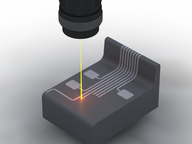
The construction of the conductor route is utilized applying the LDS approach.
LDS allows digital assemblies to be created in flexible geometric styles. Sensible telephones, hearing aids and sensible watches are becoming smaller sized and additional impressive thanks to this course of action. Resource: Harting
The additives in the materials are “activated” by immediate laser structuring so that the plastic material can accommodate the electrical conductor paths. The laser beam writes the regions supposed for the conductor paths and makes a micro-rough framework. The launched metal particles type the nuclei for the subsequent chemical metallisation. In this way, the electrical conductor paths are applied to the regions marked by the laser. The other spots of the a few-dimensional base system continue to be unchanged. The plastic ingredient can then be assembled in standard SMD processes similar to a regular PCB. It is also suited for soldering in a reflow oven.
Multipurpose application of laser technological know-how
As a person of the biggest suppliers of 3D-MID components outside of Asia, HARTING makes use of large-effectiveness laser devices for the LDS method, with a few lasers working in parallel, every offset by 45 levels. Many thanks to an added axis of rotation, elements can be processed by the laser concurrently from all sides (360 levels). This technological know-how enables versatile geometric styles, these as reflector shells or LED lights, to be manufactured. Even with the nominal conductor path thickness of 16 to 20 μm, the conductor paths are even now ideal for demanding automotive factors or for purposes with currents up to 10 A – for case in point for heating coils in cameras which are made use of to prevent the optics from fogging up
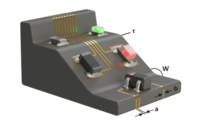
Bare minimum distances involving the conductor paths (a): 50 – 150μm. Minimal width of the conductor paths (b): 50 – 150μm Radius (r): .2mm. Source: Harting
Recurrent changes in the course of the electronics advancement section or new components with modified proportions can lead to high-priced changes through common PCB output. The laser layout, in contrast, can be tailored quite flexibly by employing the parameters of the laser’s management software program. No improvements in the injection moulding are required for this.
The generation of prototypes working with LDS is also a lot easier compared to traditional procedures. HARTING can make the plastic foundation physique employing LDS-compatible product and 3D printing. Injection moulding can also be employed with inexpensive prototype instruments.
New traits in the LDS method
A number of features of LDS engineering have been enhanced and even further made more than the earlier handful of yrs.
- The working spot of the laser has been enlarged from 160 x 160 x 80 mm to 200 mm x 200 mm x 80 mm, consequently enabling a greater packing density and the processing of even larger factors.
- The performing pace of the laser can be doubled to 4 m/s by optimizing the servo models and mirrors which guidebook the laser beam, therefore drastically cutting down the processing time.
- The improvement of the optics permits the use of a laser with a diameter of 100 μm and a laser with a fantastic concentration of 50 μm for processing even scaled-down constructions.
HARTING is the only 3D-MID company in the entire world that has a laser system with 3 fine emphasis optics of 50 μm. Even smaller conductor route gaps can be accomplished many thanks to this great concentration laser. So, many conductor paths can be created on the similar component and a higher packing density can be implemented. This is applied for safety technology, among other items, because the intently spaced and intertwined conductors are able of triggering security alarms from even the smallest bodily interference.
Advancements in components and economics
Only specially picked thermoplastics are accredited for the LDS process these are readily available from inventory. The course of action can be additional enhanced with purchaser-certain adjustments to the plastic materials:
- HARTING employs a approach which adds LDS additives to non-licensed products to make them MID-appropriate.
- Precise RAL or Pantone colors can be realized with MID plastics by employing color pigments and exclusive LDS additives.
- By picking out appropriate additives, unique RF qualities can also be carried out, relying on the frequency assortment.

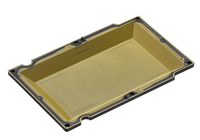
Electronic parts – these as LEDs, ICs, photodiodes and sensors – can be hooked up right onto the element carrier. The assembled component carriers can then be processed as conventional SMD elements. Source: Harting
To further make improvements to the price tag-efficiency of the producing method, HARTING relies on automatic robotic techniques. The LDS laser procedure is geared up with a rotary indexing desk so that a ingredient can be inserted or removed while a different element is still being processed. The in-feed and unloading techniques are automatic by HARTING using robotics. This will increase throughput and autonomy, whilst also enabling integration into automated output procedures. An more automation phase is presented during the injection moulding course of action. Here, too, a robotic usually takes around the elimination of the injection moulded components. The use of robotics also improves the specific reproducibility of the processes and, so, general product high quality.
Additional growth for 3D-MID
The 3D-MID caps safeguard the electronics from unauthorized access both equally mechanically and electronically. A highly exact meandering construction detects every entry, no issue how compact, and for that reason stops theft. Resource: Harting
HARTING studies enhanced need for MID tasks and has even further expanded the 3D-MID division by investing in machinery and by getting a competitor’s business. Progressive in-property products and solutions are also contributing to more advancement. HARTING has developed a option based mostly on 3D-MID technological know-how which replaces versatile PCBs with a component carrier. Alternatively of employing a flex-PCB, the element carrier can be equipped instantly with electronic elements, so conserving up to two thirds of the price tag.
—————————————-
About HARTING 3D-MID
HARTING 3D-MID is featuring the entire value chain for 3D-MID technologies from a one source, like progress/prototyping of purchaser-specific items, injection moulding, laser direct structuring, metallization, assembly and relationship technological know-how, as well as ultimate inspection. Its main business is the production of mechatronic factors for car producing, business, healthcare know-how and sensor devices.
Dirk Rettschlag, venture manager & IE MID at Harting MID.


More Stories
IMT Centre For Distance Learning
Maritime Law Assessment For Maritime Employee
Integrating Ethics Into Your Organization